Return to:
Encyclopedia Home Page –
Table of Contents –
Author Index –
Subject Index –
Search –
Dictionary –
ESTIR Home Page –
ECS Home Page
DIELECTRICS
William D. Brown,1 Dennis Hess,2 Vimal Desai,3 and M. Jamal Deen4
1Department of Electrical Engineering, University of Arkansas
3217 Bell Engineering Center, Fayetteville, AR 72701, USA
2School of Chemical and Biomolecular Engineering, Georgia Institute of Technology
311 Ferst Drive, Atlanta, GA 30332, USA
3Mechanical, Materials and Aerospace Engineering, University of Central Florida
4000 Central Florida Blvd., Orlando, FL 32816, USA
4Electrical and Computer Engineering, McMaster University
1280 Main Street West, Hamilton, ON L8S 4K1, Canada
(May, 2006)
What is a dielectric? An historical perspective
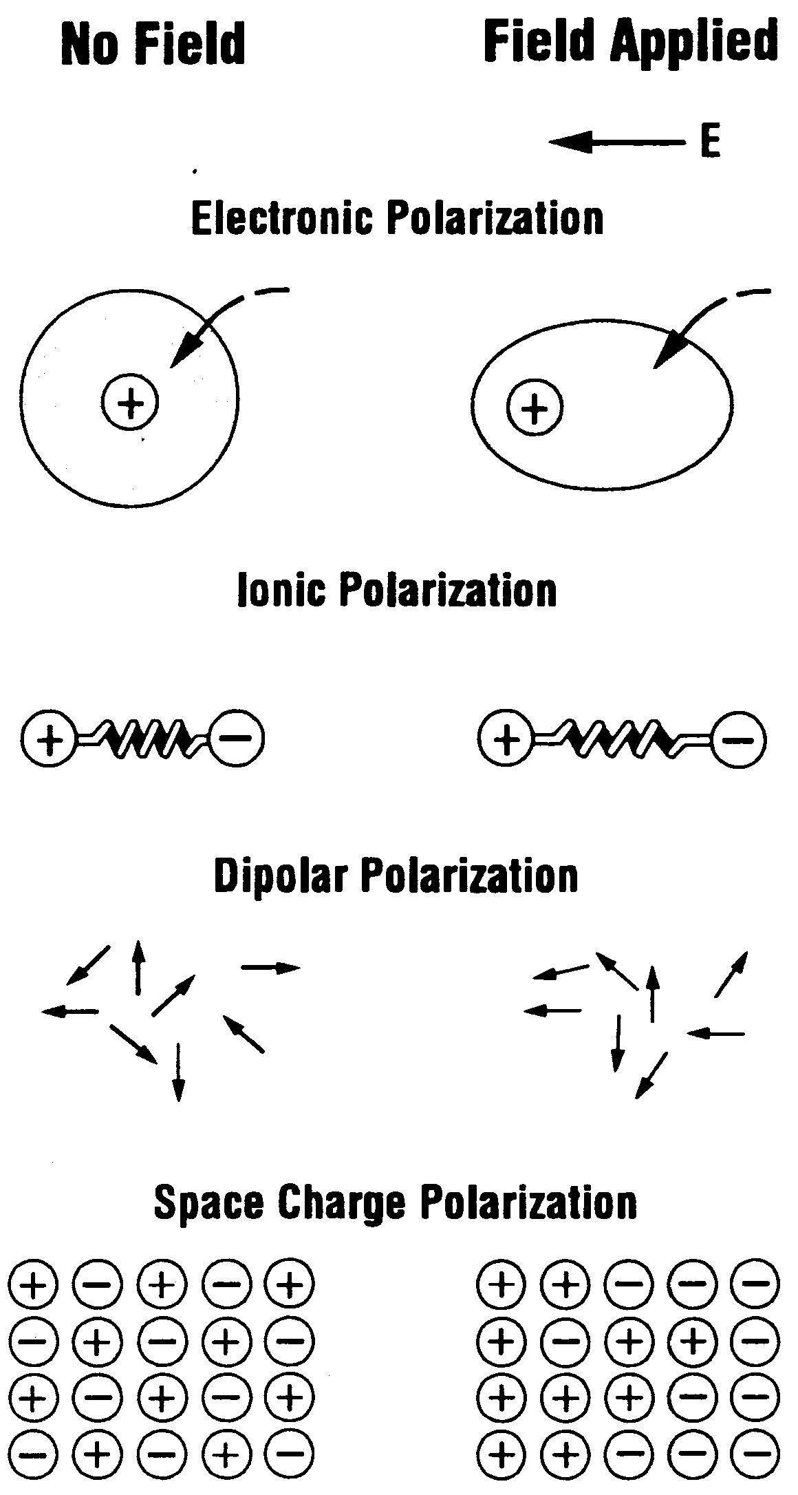
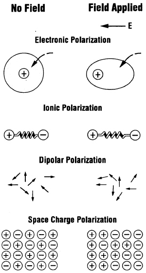 |
| Fig. 1. Schematic representation of different mechanisms of polarization. |
The science of dielectrics, which has
been pursued for well over one hundred
years, is one of the oldest branches of
physics and has close links to chemistry,
materials, and electrical engineering.
The term dielectric was first coined
by Faraday to suggest that there is
something analogous to current flow
through a capacitor structure during
the charging process when current
introduced at one plate (usually a metal)
flows through the insulator to charge
another plate (usually a metal). The
important consequence of imposing a
static external field across the capacitor
is that the positively and negatively
charged species in the dielectric become
polarized. Charging occurs only as the
field within the insulator is changing.
Maxwell formulated equations for
electromagnetic fields as they are
generated from displacement of electric
charges and introduced dielectric and
magnetic constants to characterize
different media. It is generally accepted
that a dielectric reacts to an electric
field differently, compared to free space,
because it contains charges that can he
displaced. Figure 1 illustrates some of the
charge configurations and their response
(polarization) under the influence of
an external field. Because almost all
material systems are made up of charges
(an exception being neutron stars!), it is
useful to characterize materials by their
dielectric constant.
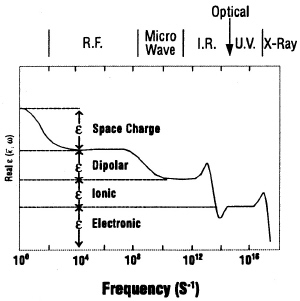 |
| Fig. 2. Contributions to the frequency-dependent dielectric constant from the different charge configurations. |
A schematic representation of
the real part of the dielectric constant is shown in Figure
2. At high frequencies (>1014 Hz),
the contribution comes solely from
electronic polarization, implying that
only free electrons, as in metals, can
respond to the electric field. That is why
metals are such good optical reflectors!
Even the various
thermal and mechanical properties, such
as thermal expansion, bulk modulus,
thermal conductivity, specific heat,
and refractive index, are related to the
complex dielectric constant, because
they depend on the arrangement and
mutual interaction of charges in the
material. Thus, the study of dielectrics
is fundamental in nature and offers a
unified understanding of many other
disciplines in materials science.
The scope of dielectric science and technology
 |
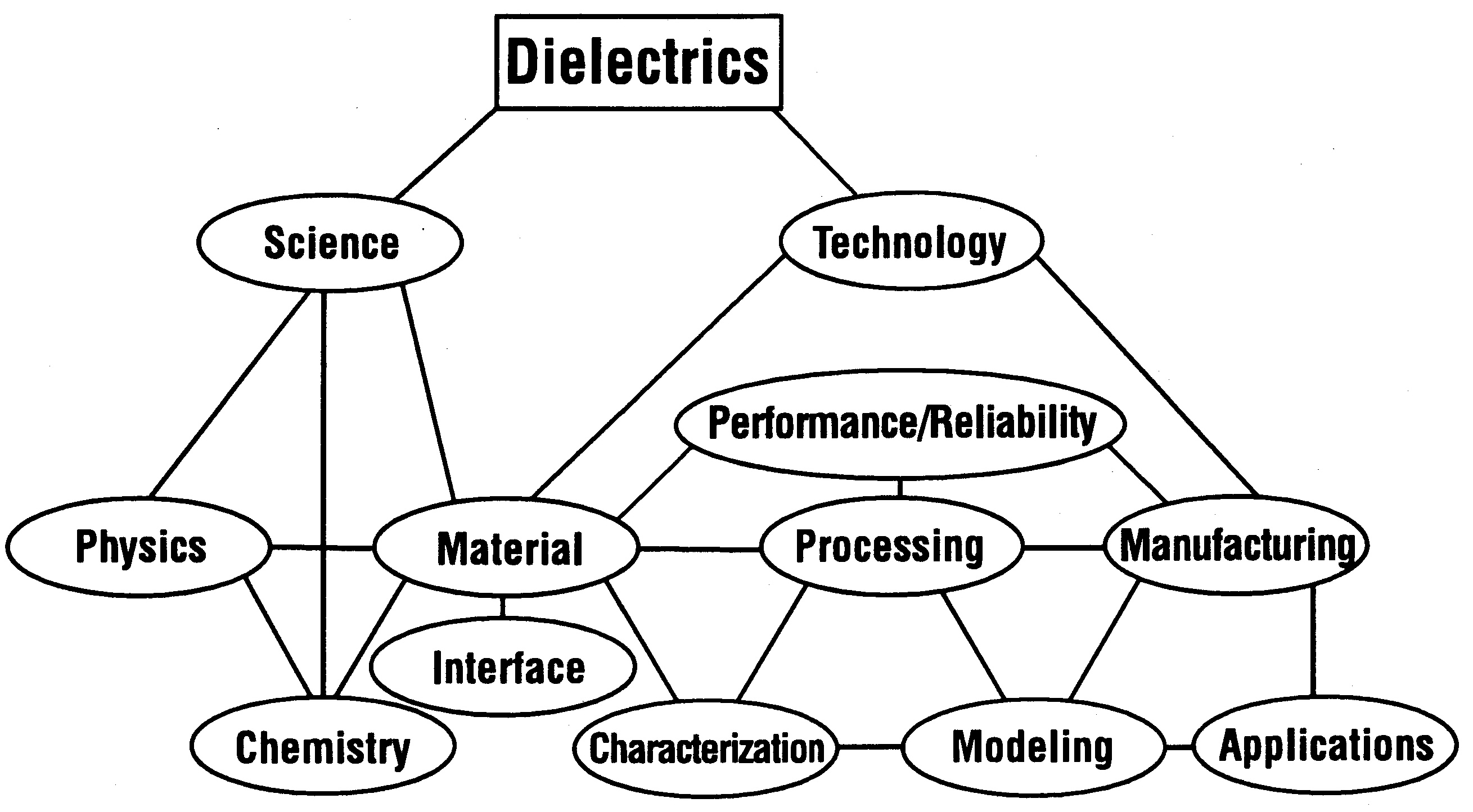
| Table I. Core Areas of Dielectric Science and Technology |
| |
| Physics/Chemistry/Materials Science |
| |
- Polarizability, Relaxation, Ions, Breakdown Phenomena
- Elementary Excitations: Polaritons, Excitons, Polarons, Phonons
- Phase Transitions, Critical Phenomena
- Bonding, Ionicity, Crystal/Ligand Fields, Electronic Correlation
- Bonding, Reaction, Kinetics, Transport, Energetics, Thermodynamics
- Interfaces, Interphases
|
| |
| Properties of Dielectrics |
| |
- Structural/Mechanical
- Thermal
- Electrical
- Optical
- Magnetic
- Chemical
|
| |
| Synthesis/Processing |
| |
- Deposition: Chemical Vapor Deposition CVD, Plasma-CVD, Room Temperature (RT)CVD, Physical Vapor Deposition (PVD), Sputtering. Evaporation, Dip/Spin/Spray Coating
- Growth: Thermal, Anodic, Epitaxial
- Chemical Mechanical Planarization (CMP)
- Lithographic Processes: Photon/ Election/Ion Beam Exposure, Resist Materials
- Etching: Wet Chemical, Plasma, Reactive Ion, Ion Beam Milling Characterization
- Analytical Tools
- Modeling Manufacturing
- Monitoring/Control
- Yield
- Statistical Analysis
|
| |
| Reliability |
| |
- Failure Mode Analysis
- Performance Prediction
- Quality Assurance Applications
- Structural/Transportation
- Microelectronics/Optoelectronic
- Corrosion and Passivation
- Energy Production and Storage
|
| |
In time, the focus on dielectric science and technology has broadened from the
materials of
the traditional dielectric films used in
semiconductor devices and capacitors,
particularly oxides and nitrides.
More recently, materials of
unique dielectric responses have been
studied and utilized in novel ways.
Table I lists many
of the core technology areas of interest to
those involved in dielectric science and
technology.
For instance, in the not too distant
past, polymer scientists and technologists
expanded their horizons from consumer
products to the high technology arena.
Particularly notable are inventions in
telecommunications, where plastic
fibers are used for short optical data
links, and polymeric films are used
for nonlinear optics applications. In
the field of microelectronics, radiation
sensitive polymers (photoresists) have
been formulated for use with a wide
variety of exposure systems, from the
early ones using visible light to those
using near ultraviolet, laser, e-beam, and
x-ray sources, for the fabrication of the
sub-micrometer structures of high speed,
high density integrated circuits. Steady
progress has also been made in the field
of passivation, where various polymeric
films are applied to microscopic objects
such as integrated circuits and the
packages that house them.
Ceramists have also extended
the range of applications; ceramic
materials are used in packages for
semiconductor integrated circuits, as well
as in automobile engines, in composites
for aerospace vehicles, and in high
efficiency power generation stations. A
notable advance was the discovery of
high-temperature superconductivity, for which Bednorz and
Muller were awarded the Nobel Prize in
Physics in 1987.
Electronic and optical engineers
are pushing the limits of the material
properties and applications of
organic and inorganic conductors,
semiconductors, and insulators. One
example is the revived interest in
diamond and diamond-like films.
These recent efforts resulted in
higher speed, higher density devices
and interconnection schemes, both
electrical and optical, for computers and
telecommunication systems. Another
example, the low-dimensional (d = 1,
2) nanostructures, which could only be
speculated about in the past, are now
a reality. This allows researchers to test
some fundamental concepts in quantum
mechanics. It is
probable that more innovative devices
will follow.
Since the mid-1990s, the
microelectronics industry has invested
heavily, with some success, in the
development of high- and low-k
dielectrics (�k� is the dielectric constant of
a material). These materials are required
because of the continuing reduction of
both horizontal and vertical dimensions
of integrated circuits (ICs), which results
in an increase of the gate leakage current,
and consequently, an increase in heat
dissipation. Therefore, high-k materials
are needed for the gate dielectric in
complementary metal-oxide-semiconductor (CMOS) ICs, storage capacitors,
and nonvolatile static memory devices.
Similarly, the reduction in spacing of
metal interconnects in both the vertical
and horizontal dimensions has created
the need for low-k materials that serve as
interlevel dielectrics to offset the increase
in signal propagation time between
transistors, known as RC delay (�R� is
metal wire resistance and �C� is interlevel
dielectric capacitance). As a result of
these requirements for present and future
sub-100 nm IC technologies, many
new dielectric materials and material
combinations have been and must
continue to be created and characterized
if the device density of ICs is to continue
to increase as anticipated by Moore�s
Law.
The previous discussion is not
intended to suggest that dielectric
science and technology is only important
for electronic components. Far from
it; dielectrics play important roles
in applications ranging from sensors,
isolation for conductors in the power
utility industry, to ceramic cookware.
Further, in the rapidly emerging field of
biological systems, the dielectric constant
is important because electrostatic effects
are used to link the structure and function
of biological molecules. It has been
proposed that electrostatic effects play
a major role in important biological
activities such as enzyme catalysis,
electron transfer, proton transport, ion
channels, and signal transduction. The role of the science and technology of
dielectrics is also important in existing fields of sensors,
nanotechnology, electronics, photonics,
chemical and mechanical systems, and in emerging fields of biology and
biochemistry. Thus, it appears inevitable
that the dielectric properties of nanoscale
materials and structures will be critical
to developing novel devices for current
and future commercial applications.
For example, large amounts of energy
can be stored in nanocomposites that
show large polarizabilities. In addition,
dielectric materials such as ferroelectric
and piezoelectric nanomaterials
offer significant advantages for
communication devices and data
storage systems. Recently, there have
been investigations of nanoporous
composites formed by the incorporation
of nanosize air bubbles, leading to a
significant decrease in the dielectric
constant and the ability to vary the
dielectric constant by controlling
the concentration of air bubbles.
Furthermore, the continuing trend in
miniaturization requires increasingly
thinner dielectric materials without
nanoscale defects. An understanding of
material and interfacial properties at the
nanoscale is often facilitated by materials
modeling as well as the development
of innovative characterization tools.
One such tool is the development of the
scanning nonlinear dielectric microscope
(SNDM) that can be used to measure
the microscopic point-to-point variation
of the linear and nonlinear dielectric
properties of insulators.
Future requirements and achievements
in the area of dielectrics can be realized
only by the further development and
fundamental understanding of reliable
material synthesis, processing, and
characterization technologies, making
it possible to tailor dielectric materials,
their thin film structures, and their
interfaces to specific applications.
In the past, these technologies have
been successfully applied in the
microelectronics and other industries
that depend on the unique mechanical,
optical, chemical, and electrical
properties of high performance dielectric
materials. The advent of nanoscale
devices in recent years demands that
scientists and engineers continue to
focus attention on dielectric material
design, synthesis, and characterization
for enhanced performance, reliability,
and manufacturability.
 |
| Fig. 3. Interactions among the core areas of dielectric science and technology. |
Figure 3 is an attempt to depict
the multitude of interactions among
the many and diverse core areas of
dielectric science and technology
that present challenging possibilities
for the community of scientists,
engineers, and technologists in research,
development, and manufacturing.
Acknowledgement
This article was reproduced from The Electrochemical Society Interface (Vol. 15, No. 1, Spring 2006) with permission of The Electrochemical Society, Inc. and the authors.
Bibliography
- Material Science and Engineering for the 1990s, National Academy of Science Press, Washington, 1989.
- Introduction to Ceramics (2nd edition), W. D. Kingery, H. K. Bowen, and D. R. Uhlmann, pp 918 et seq., Wiley, New York, 1976.
- Introduction to Solid State Physics (4th edition), C. Kittel, Wiley, New York, 1971.
- Solid State Physics, Advances in Research and Applications, F. Seitz, D. Turnbull, and H. Ehrenreich, Academic Press, New York, 1969.
- Theory of Quantum Liquids, D. Pines and P. Nozieres, p. 280, Benjamin, New York, 1966.
Listings of electrochemistry books, review chapters, proceedings volumes, and full text of some historical publications are also available in the Electrochemistry Science and Technology Information Resource (ESTIR). (http://knowledge.electrochem.org/estir/)
Return to:
Top –
Encyclopedia Home Page –
Table of Contents –
Author Index –
Subject Index –
Search –
Dictionary –
ESTIR Home Page –
ECS Home Page
|