Return to:
Encyclopedia Home Page –
Table of Contents –
Author Index –
Subject Index –
Search –
Dictionary –
ESTIR Home Page –
ECS Home Page
ATOMIC LAYER DEPOSITION BY ELECTROCHEMISTRY
John L. Stickney
Department of Chemistry, University of Georgia
Athens, GA 30602, USA
(June, 2012)
Electrodeposition has served as a thin film preparation method since the 19th century, though it is thought
by some to be more prone to contamination and less
precise than corresponding vacuum processes. With the
introduction of the electrodeposition process for the formation
of interconnects in ultra large scale integration (ULSI), it has
become clear however that electrodeposition can be as clean
as any other thin film deposition technique. This article
argues that electrochemical atomic layer deposition (E-ALD)
can control deposition down to the single atomic layer, and may someday rival molecular beam epitaxy (MBE) for control
in nanofilm growth. This article discusses the
principles on which electrochemical atomic layer deposition is based and the technological opportunities it provides.
Atomic layer deposition (ALD) is a methodology for
forming nanofilms of materials one atomic layer at a time using
surface limited reactions. Surface limited reactions occur only at the substrate
or deposit surface: once the surface (the limiting reagent) is
covered the reaction stops. �Electrochemical atomic layer deposition� (E-ALD or EC-ALD and ECALD) is atomic layer deposition in an electrochemical
environment. Various other names have also been used for electrochemical atomic layer deposition, including �electrochemical atomic layer epitaxy� (EC-ALE or
ECALE). Electrochemical atomic layer deposition is based on underpotential deposition (UPD), which is a type of electrochemical surface limited reaction, where an atomic layer of an element is deposited on the surface, using an electrochemical cell, at an electrode potential lower that needed to deposit the element on itself. This is caused by an energetic effect, where the interaction energy between the element deposited and the surface is larger than the interaction of the element with itself, thus resulting in the formation of a
surface compound or alloy with some energy saving.
The term �atomic layer� refers to a coverage less than a monolayer
(ML), a monolayer being a unit of coverage particular to the deposit
being formed. From a surface chemistry point of view, a monolayer is
formed when there is one deposit atom for each surface atom, at which point the deposition stops. It is possible to produce on the top of this layer another monolayer of a different element, and so on, if the energetics are favorable. A more detailed discussion of this energetics effect and the reactions occurring in the example described below are available in the Appendix.
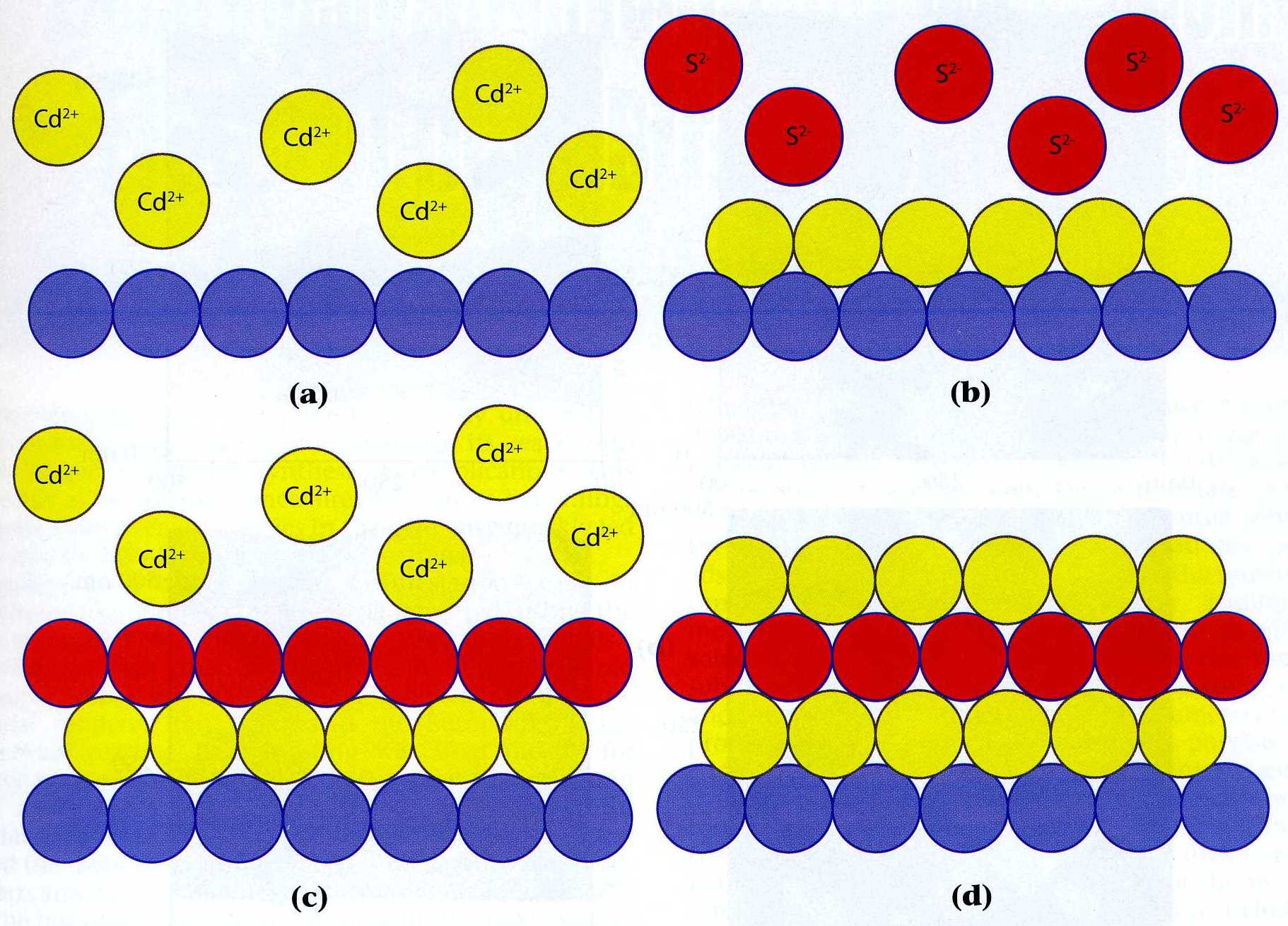 |
| Fig. 1. Scheme for a cadmium sulfide E-ALD cycle. (a) exchange for cadmium ions, (b) cadmium reductive UPD and exchange for sulfide ions, (c) sulfide oxidative UPD and exchange for cadmium again, (d) one and a half bi-layers of cadmium sulfide. |
Each pair of elements has its own UPD chemistry, which
must be investigated to devise an electrochemical atomic layer deposition cycle. Such a cycle is the sequence of steps used to deposit one stoichiometric layer
of the desired material: this would be an atomic layer for a
pure element, or a bi-layer of a 1:1 compound. The cadmium sulfide electrochemical atomic layer deposition
cycle (Figure 1) is an illustrative example: initially an atomic layer of cadmium is
deposited followed by an atomic layer of sulfur
deposition on the cadmium, and one of cadmium is again deposited on the sulfur.
The cycle is composed of several steps: a reductive underpotential deposition of cadmium
from a cadmium cation solution, a blank rinse, oxidative underpotential deposition of sulfur
from a sulfide anion solution, a blank rinse, a second reductive underpotential deposition of cadmium
from a cadmium cation solution, and one more blank rinse. Separate
solutions are used for each reactant and different potentials for each cycle step. The use of separate solutions and potentials
provides extensive control over deposit growth, composition,
and morphology. A cycle is repeated to form a nanofilm, with
the deposit thickness being a linear function of the number of
cycles. This linear growth is a good indication of a layer by layer
mechanism, and an atomic layer deposition process.
There are a number of cycle chemistries that can be
applied, depending on the depositing elements. The cadmium sulfide
cycle is an oxidative-reductive UPD cycle (O-R). In practice,
few compounds can be formed using O-R, because of a lack of
suitable negative oxidation state precursors (like the sulfide anion), for which
oxidative UPD is practicable. Other cycle chemistries include:
reductive-reductive UPD (R-R), R-R with a reductive strip
(R-R-R), R-R with an oxidative strip (R-R-O), bait and switch
(B&S), and surface limited redox replacement (SLRR).
To achieve compound formation, the applied potentials and
solution compositions for the electrochemical atomic layer deposition cycle should be optimized, resulting in a stoichiometric ratio of atomic layer coverages
each cycle. As long as deposits are formed at underpotentials,
the inherent stability associated with the formation of a
stoichiometric compound will control the atomic layer
coverages. For a binary compound like cadmium sulfide, the atomic layer
coverages will be identical, after the first few cycles. The
amounts of an element deposited during each cycle will be a
function of the potential chosen. The farther the underpotential deposition potential
is from then equilibrium potential (that is, the larger the underpotential), the less of that element that will deposit. In turn, less of the second element will deposit, since its deposition is limited by the availability
of the first element on the surface. Stoichiometric cadmium sulfide will still
result, but the growth will be at a lower rate (nm/cycle).
The above discussion suggests that each cycle results in a
conformal compound layer, deposited over the whole surface.
The rules for thin film formation still apply, however. Lattice
matching with the substrate, for instance, is still an issue, and
strain will increase as the number of cycles increases. Strain
will be released when the critical thickness is achieved, with
the formation of threading dislocations and other defects.
The substrate may be a single crystal, wafer, polycrystalline
film, foil, or powder. Each crystallographic facet will have a
different affinity for the depositing element, and will result in a
different coverage and interface structure. When various facets
coalesce, grain boundaries will form, and the cycle conditions
chosen will determine the resulting deposit morphology. Use
of more aggressive conditions (smaller underpotentials) could
cause roughening at grain boundaries, while use of larger
underpotentials could minimize deposition at the boundaries
(Figure 2). Even when a single crystal is used as a substrate, there
will be steps and defects, which may nucleate different deposit
structures and orientations. The first electrochemical atomic layer deposition cycle is performed on the substrate, generally a different material. The optimal
deposition conditions for the first few cycles may thus differ
from the steady state conditions used to grow the remaining
nanofilm, where the compound deposits on itself.
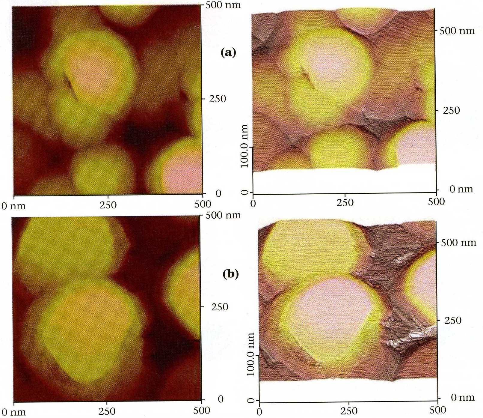 |
| Fig. 2. Scanning tunneling microscopy images: (a) gold vapor deposited on glass; (b) 30 superlattice periods, each consisting of 3 cycles of lead selenide, followed by 15 cycles of lead telluride, on the gold
vapor deposited on glass. Note the nearly atomically flat terraces resulting from the E-ALD deposit. |
One of the major differences between electrochemical atomic layer deposition and the
various vacuum and gas based deposition methodologies,
besides use of a condensed phase, is temperature. Electrochemical atomic layer deposition is performed at room temperature or under the boiling point of
the solvent, all of which are considered �low temperature� for
thin film formation. Despite formation at �low temperature,�
the deposits form under equilibrium conditions. The
deposition potential is applied until the current goes to zero and the composition and structure are constant, indicating
that equilibrium has been reached for that potential. This is made possible by the exchange current. Electrochemical deposition is a dynamic process, where atoms are depositing and dissolving at the same time. The measured current is
the difference between the deposition and dissolution flux,
and when it is zero, equilibrium has been established. The exchange current
is a measure of the rate at which atoms are depositing and dissolving, at equilibrium. Ideally, atoms in high energy sites are dissolving and redepositing in more stable sites. The result
is similar to thermal annealing, or to surface diffusion, in gas
or vacuum phase thin film deposition methods. Several other
electrodeposition methodologies benefit from depositionat potentials near equilibrium; however, many involve
overpotential deposition, where the contribution of exchange current is insignificant, so that deposited atoms tend not to redissolve,
and deposits become disordered.
An increasing number of groups around the world have
been using electrochemical atomic layer deposition to form a wide variety of materials for a wide variety of applications. Different nanofilms are formed
for infrared detector materials, thermoelectric materials, and photovoltaic materials.
Most electrochemical atomic layer deposits are formed using some type of
electrochemical flow cell that allows for the rapid exchange of solutions, in combination with automation, the cycle can be programmed, and
allowed to run for as many cycles as desired. Graduate students
manually performing cycles usually tire and make mistakes
somewhere after the 10th cycle. The more elements involved
in the deposit, the more solution lines are required. More
complex sequences of potentials and solution exchanges can be performed as well, such as the formation of a superlattice
where two or more materials are alternated to form materials
with unique lattice constants, and optical and electronic properties (Figure 2).
Appendix
In electrodeposition, the metal ion reduction to the element,
[1]  M2+ + 2 e- ==> M M2+ + 2 e- ==> M
is generally controlled by the applied potential, which is dictated by
the activity ratio of products to reactants according to the
Nernst equation:
[2] 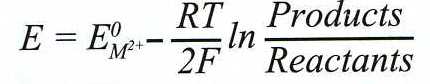
Conventionally, the product is a bulk metal with an activity of
unity. In underpotential deposition, however, the product is an atomic layer, which
has a different electronic structure than the bulk metal, due to its interaction with the substrate. The activity of the product
is then less than unity, shifting the equilibrium potential, and accounting for underpotential deposition, which occurs when the depositing element is more stable on the substrate than on itself. Underpotential deposition is fundamentally an surface limited reaction, as long as the applied potential is under the potential for bulk deposition, in the given
solution. Bulk deposits do not form at an underpotential,
regardless of the deposition time.
The reactions occurring in the example shown in Figure 1 are:
[3] Cd2+ + 2 e- ==> CdUPD
[4] S2- ==> SUPD + 2 e-
Acknowledgements
This article was reproduced from The Electrochemical Society Interface (Vol. 20, No. 2, pp 28-30, Summer 2011) with permission of The Electrochemical Society, Inc. and the author.
Related article
Electroplating
Bibliography
- Electrodeposition of Compound Semiconductors by Electrochemical Atomic Layer Epitaxy (EC-ALE), J. L. Stickney, T. L. Wade, B. H. Flowers, R. Vaidyanathan, and U. Happek, in �Thermodynamics and Electrified Interfaces� (Encyclopedia of Electrochemistry, Vol. 1) pp 513-560, E. Gileadi and M. Urbakh (editors), Wiley-VCH, Weinheim, Germany, 2002.
- Electrochemical Atomic Layer Epitaxy (EC-ALE): Nanoscale Control in the Electrodeposition of Compound Semiconductors, J. L. Stickney, in �Advances in Electrochemical Science and Engineering� Vol. 7, pp 1-105, R. C. Alkire and D. M. Kolb (editors), Wiley-VCH, Weinheim, Germany, 2002.
- Electrochemical Atomic Layer Epitaxy, J. L. Stickney, in �Electroanalytical Chemistry: a Series of Advances� Vol. 21, pp 75-210, A. J. Bard and I. Rubinstein (editors), Marcel Dekker, New York, 1999.
- Epitaxial Compound Electrodeposition, T. L. Wade, T. A. Sorensen, and J. L. Stickney, in �Interfacial Electrochemistry: Theory, Experiment and Applications� pp 757-768, A. Wieckowski (editor), Marcel Dekker, New York, 1999.
Listings of electrochemistry books, review chapters, proceedings volumes, and full text of some historical publications are also available in the Electrochemistry Science and Technology Information Resource (ESTIR). (http://knowledge.electrochem.org/estir/)
Return to:
Top –
Encyclopedia Home Page –
Table of Contents –
Author Index –
Subject Index –
Search –
Dictionary –
ESTIR Home Page –
ECS Home Page
|